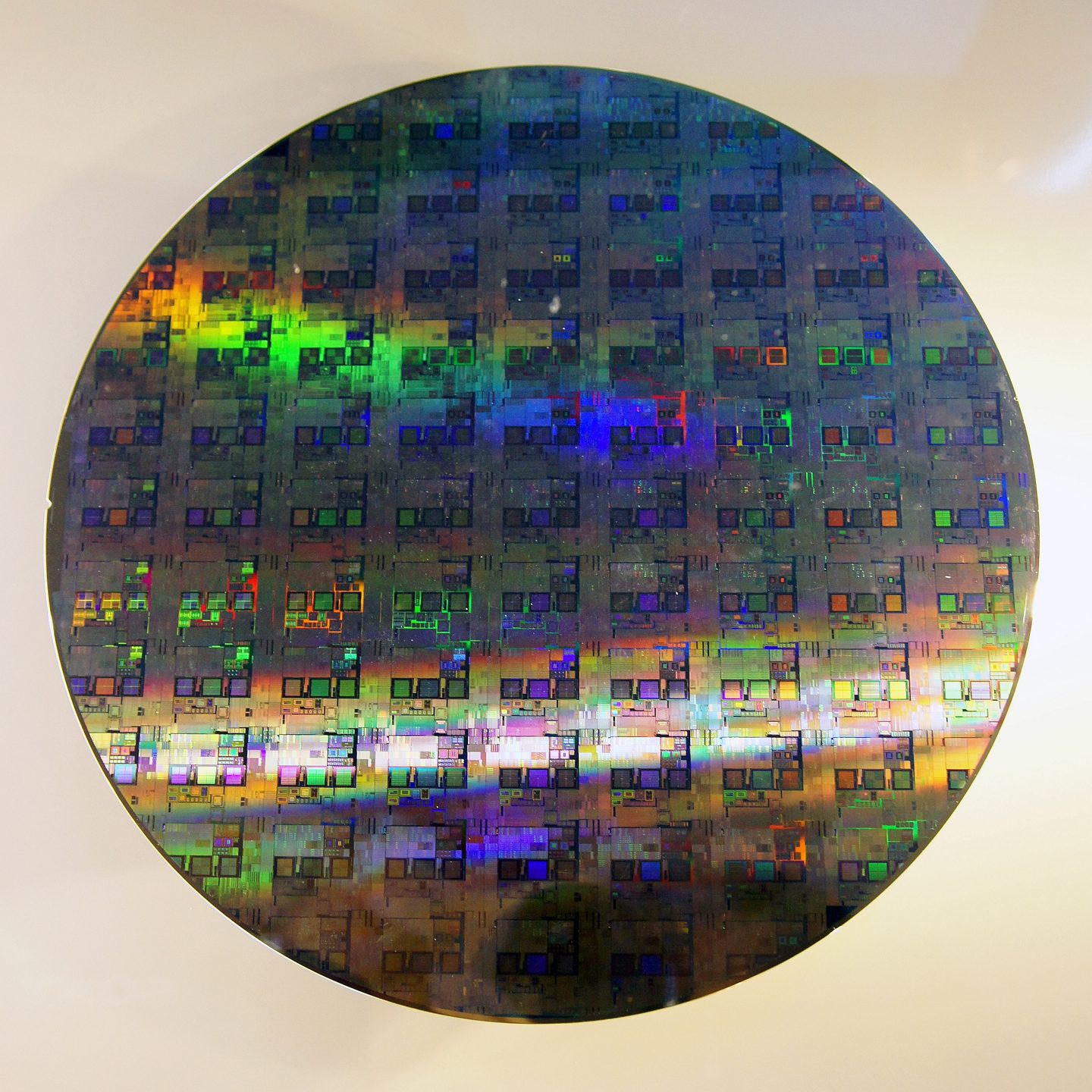
EUV lithography — extreme ultraviolet lithography — is the manufacturing process that etches the microscopic circuit patterns onto the silicon chips inside every advanced AI processor. It works by firing a laser at droplets of molten tin 50,000 times a second to generate light with a wavelength of just 13.5 nanometers, then bouncing that light off a chain of ultra-precise mirrors onto a wafer coated in a light-sensitive chemical. Only one company in the world builds machines that can do this at production scale — the Dutch firm ASML — which turns a manufacturing step into a geopolitical chokepoint: whoever can buy an EUV machine can make cutting-edge AI chips; whoever can’t, can’t.
What lithography actually does
Making a chip means printing dozens of layers of circuitry onto a silicon wafer, one on top of the other, each only a few atoms thick. Photolithography is how that printing happens: light passes through a stencil-like mask carrying the circuit pattern, then focuses onto the wafer’s light-sensitive coating, hardening it wherever the light lands. An etching step then removes everything the light didn’t touch, leaving the pattern in silicon. Repeat that dozens of times, align every layer to a fraction of a nanometer, and the result is a chip carrying billions of transistors.
The smallest feature a lithography machine can print is limited by the wavelength of the light it uses — shorter wavelengths draw finer lines. For three decades, chipmakers used deep ultraviolet (DUV) light at a 193-nanometer wavelength, squeezing ever-smaller features out of it with tricks like multi-patterning, where the same layer is exposed several times, each pass offset slightly from the last. By the mid-2010s, that squeezing was running out of room.
How EUV closes the gap
ASML’s EUV tools use light with a 13.5-nanometer wavelength — more than 14 times shorter than DUV — letting a single exposure print features that would otherwise need several DUV passes. The catch is that EUV light is absorbed by almost everything, including air and ordinary glass lenses, so the whole process runs inside a vacuum and uses mirrors instead of lenses. Generating the light is its own feat of engineering: a laser strikes a falling droplet of molten tin twice, vaporizing it into a plasma that gives off EUV light, which curved mirrors then collect and relay onto the wafer. A standard production EUV system costs roughly $220 million; ASML’s newer High-NA variant, which prints even finer features, runs around $380-400 million per machine, as of 2026.
Why one company decides who can build AI chips
Every advanced AI chip — Nvidia’s GPUs, Google’s TPUs, Apple’s processors — is designed by one company but physically printed by a chip foundry like TSMC or Samsung, and those foundries can only print what their lithography tools allow. Since ASML is the sole source of EUV machines, and EUV is what current leading-edge chip nodes require, the company’s annual shipping schedule effectively caps how much advanced AI compute the whole industry can produce in a given year.
That chokepoint is also why EUV sits at the center of AI chip export controls. The Dutch and US governments have barred ASML from selling EUV machines to China since 2019, arguing that unrestricted access would let Chinese firms build the chips that power both AI systems and military applications. China cannot legally buy an EUV machine at any price.
In the news
Locked out of EUV, Chinese toolmakers have instead pushed to master the older DUV technology domestically. In late July 2026, reports emerged that Chinese firms had begun mass-producing homegrown DUV lithography systems and installing them at foundries including SMIC — with output still limited to a handful of machines a year and a wide performance gap left to close before they can match ASML’s imported tools.