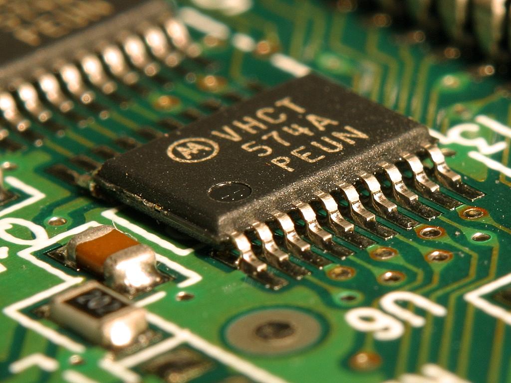
An application-specific integrated circuit, or ASIC, is a chip designed and physically wired to do one job — and only that job — as efficiently as possible. In AI, that job is usually running a specific kind of neural network, most often the transformer architecture behind today’s chatbots. Unlike a general-purpose processor, an ASIC can’t be reprogrammed to do something else once it leaves the factory: its circuitry is etched in silicon around one narrow task, which is exactly what makes it faster and more power-efficient at that task than a chip built to handle anything.
What Makes a Chip an ASIC
Every chip is a trade-off between flexibility and efficiency. A CPU is the most flexible: it can run almost any software, one instruction at a time, but that generality costs speed. A GPU sits in the middle — it was built to run thousands of similar graphics calculations in parallel, and that same parallel design turned out to suit the matrix math behind AI. An ASIC goes further: instead of general-purpose parallel cores, its transistors are laid out for one specific calculation, with no spare circuitry for anything else. Google’s Tensor Processing Unit (TPU), introduced in 2015 for its own data centers, was one of the first widely known AI ASICs — built specifically for neural-network math rather than graphics.
How an ASIC Differs From a GPU
The practical difference shows up when the workload changes. A GPU’s cores are programmable — the same chip that renders a video game can also train a language model or switch to a different kind of AI job tomorrow, because software tells it what to compute. An ASIC’s logic is fixed at the design stage, months or years before it ships. That specialization pays off in raw efficiency: with no circuitry wasted on tasks the chip will never do, an ASIC can process its one target workload faster and on less power than a general-purpose GPU handling the same task. The cost is versatility. A GPU can be repointed at a new model architecture with a software update; an ASIC generally cannot.
Why AI Companies Are Betting on ASICs
For most of the current AI boom, GPUs — led by Nvidia — have been the default hardware, precisely because their flexibility let them run whatever new model architecture researchers came up with next. But as the transformer architecture has come to dominate nearly every major AI model, that flexibility increasingly looks like wasted overhead. A growing number of companies in the AI chip industry are betting that hardwiring a chip around transformers specifically — and giving up the ability to run anything else — is worth the resulting gains in speed and power efficiency. That’s the bet behind Google’s TPU and behind newer entrants building dedicated inference chips, including startup Etched’s Sohu chip, which runs only transformer models and cannot run other kinds of AI workloads at all.
The Trade-off: Speed for Flexibility
That bet is also the risk. Designing custom silicon can cost hundreds of millions of dollars before a single chip ships, so an ASIC maker is wagering that the architecture it built around will keep dominating for years — long enough to earn that investment back. If a fundamentally different architecture displaces transformers, a chip built only for transformers becomes far less useful, while a GPU can simply run the new architecture instead. That’s why most large AI labs and cloud providers still buy GPUs as their general-purpose base, and add ASICs only for specific, high-volume workloads they’re confident will stay stable.
In the News
The trade-off is playing out in real time: Etched, the startup behind the Sohu chip, is reportedly in talks for a $20 billion valuation — a bet by investors that specialized AI silicon has a lasting place alongside general-purpose GPUs.