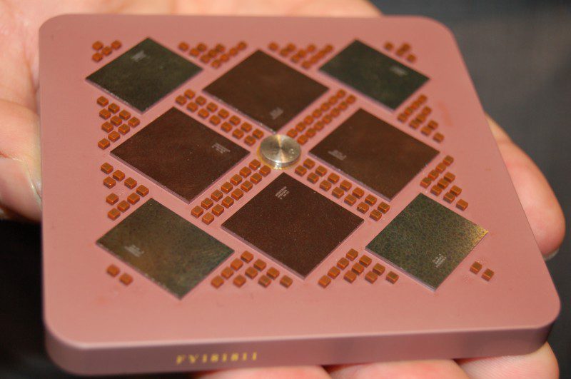
Advanced packaging is the manufacturing step that fuses several separately made silicon dies — a processor and its memory chips, for instance — into one finished chip, instead of building everything on a single slab of silicon. For today’s AI accelerators it has become almost as important as the transistors themselves, because it determines how fast data can move between compute logic and memory. It has also become the industry’s tightest bottleneck: chipmakers now compete for packaging capacity as fiercely as they compete for the chips themselves.
From afterthought to bottleneck
For decades, “packaging” was the simple, unglamorous last step in chipmaking: take a finished die off the wafer, seal it in plastic or ceramic, and attach the pins that let it plug into a circuit board. The real engineering happened earlier, at the semiconductor foundry that etches transistors onto a silicon wafer.
That division has broken down. Modern AI chips grew too large, too power-hungry, and too expensive to build as a single giant die, so chipmakers turned to advanced packaging: splitting a processor into smaller pieces — chiplets — and reassembling them inside the package itself. Packaging stopped being the box a chip ships in and became part of the chip’s actual architecture.
How the pieces get stacked
In a typical AI accelerator, several dies sit side by side or stacked on top of a base layer called an interposer — a thin slice of silicon etched with thousands of microscopic wiring channels. Chiplets, such as separate compute and I/O dies, connect to the interposer through tiny copper connections, while the interposer itself is wired down through the package with through-silicon vias — vertical channels bored straight through the silicon.
Right next to the compute die sit stacks of High Bandwidth Memory, memory chips built by stacking layers of DRAM on top of one another. Because those stacks sit millimeters from the compute logic instead of across a circuit board, the connection between them can be thousands of wires wide, moving far more data per second than memory soldered onto a motherboard ever could. That short, dense connection is the entire point: modern AI models are often limited less by how many calculations a chip can perform than by how fast it can be fed data — a constraint engineers call the memory bandwidth wall.
Why packaging, not fabrication, is the choke point
Nearly every current AI GPU — Nvidia’s H100, H200, B200, and GB200 among them, and AMD’s MI300 and MI400 — ships this way, as do the custom AI chips that Google, Amazon, and Microsoft design for their own data centers. That demand has turned advanced packaging into scarce, heavily booked capacity. Taiwan’s TSMC, which pioneered the leading process (called CoWoS, for chip-on-wafer-on-substrate), has reportedly expanded that capacity by roughly 80% a year and still cannot keep up with orders; industry reporting puts Nvidia’s reservations alone at more than half of TSMC’s CoWoS output through 2027.
The practical effect is that a chipmaker can have plenty of finished processor dies in inventory and still be unable to ship a finished AI accelerator until packaging capacity opens up. Wafer fabrication, once the industry’s defining constraint, can in principle be expanded by building more fabs; advanced packaging lines take just as long to build and are far more concentrated among a handful of suppliers, so a shortfall there ripples through the entire AI hardware market — it is one reason high-end AI accelerators stay scarce and expensive even when factories elsewhere are running at capacity. That’s why rivals are racing to build alternatives: Samsung with its Cube-series packaging lines, and Intel with EMIB and Foveros.
In the news
That race is the backdrop to Samsung’s new $200 billion supply agreement with Broadcom, which explicitly spans memory, chip fabrication, and packaging together rather than just one of the three. It gives Broadcom’s custom AI chips — the kind it designs for Google and other large customers — a second source of advanced packaging capacity beyond TSMC, alongside next-generation HBM4E and HBM5 memory and sub-2-nanometer manufacturing.
Sources: CNBC and Fortune on the Samsung–Broadcom agreement; DigiTimes on TSMC CoWoS capacity growth; Samsung Foundry’s own documentation of its Cube-series packaging.